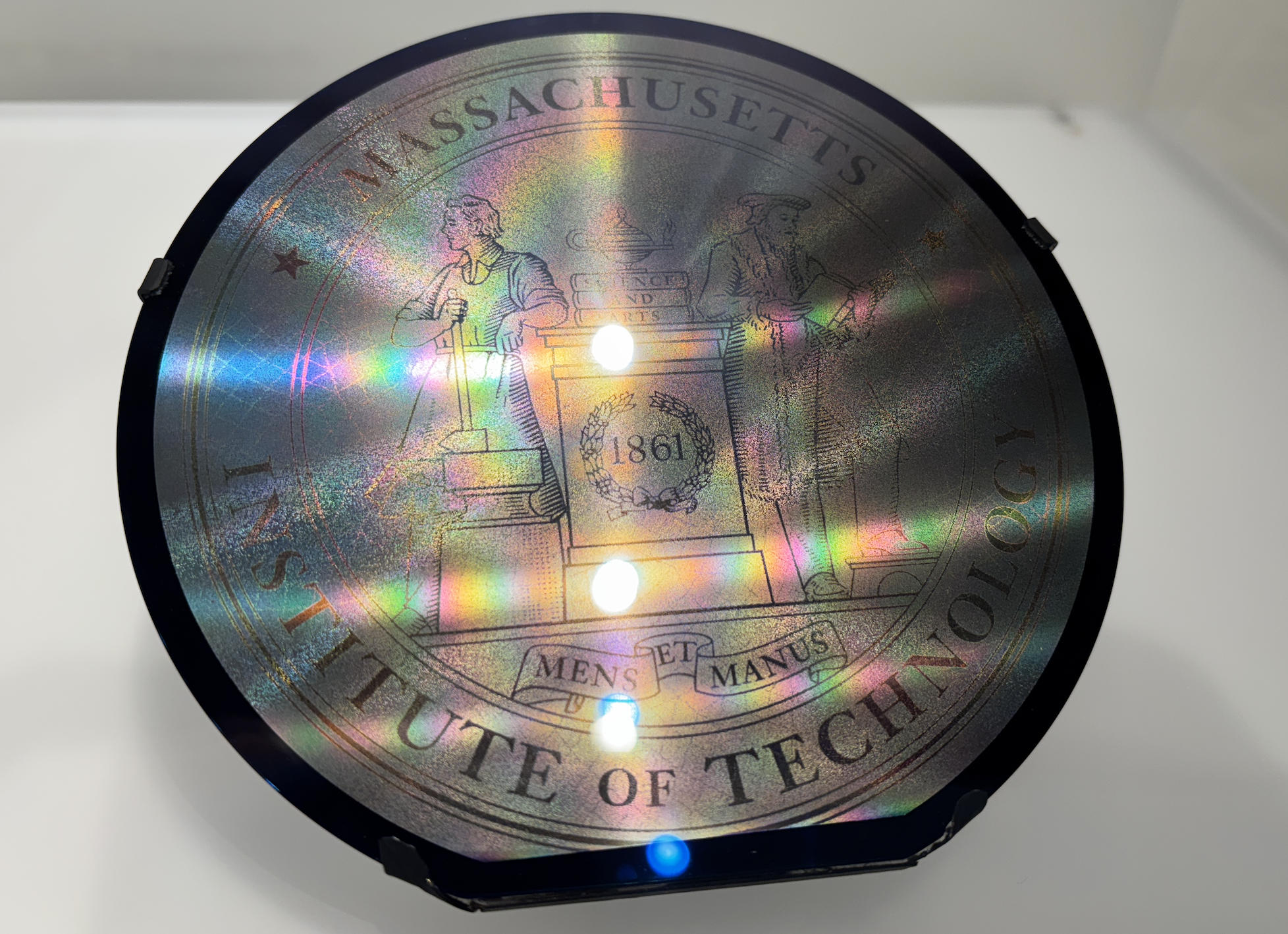
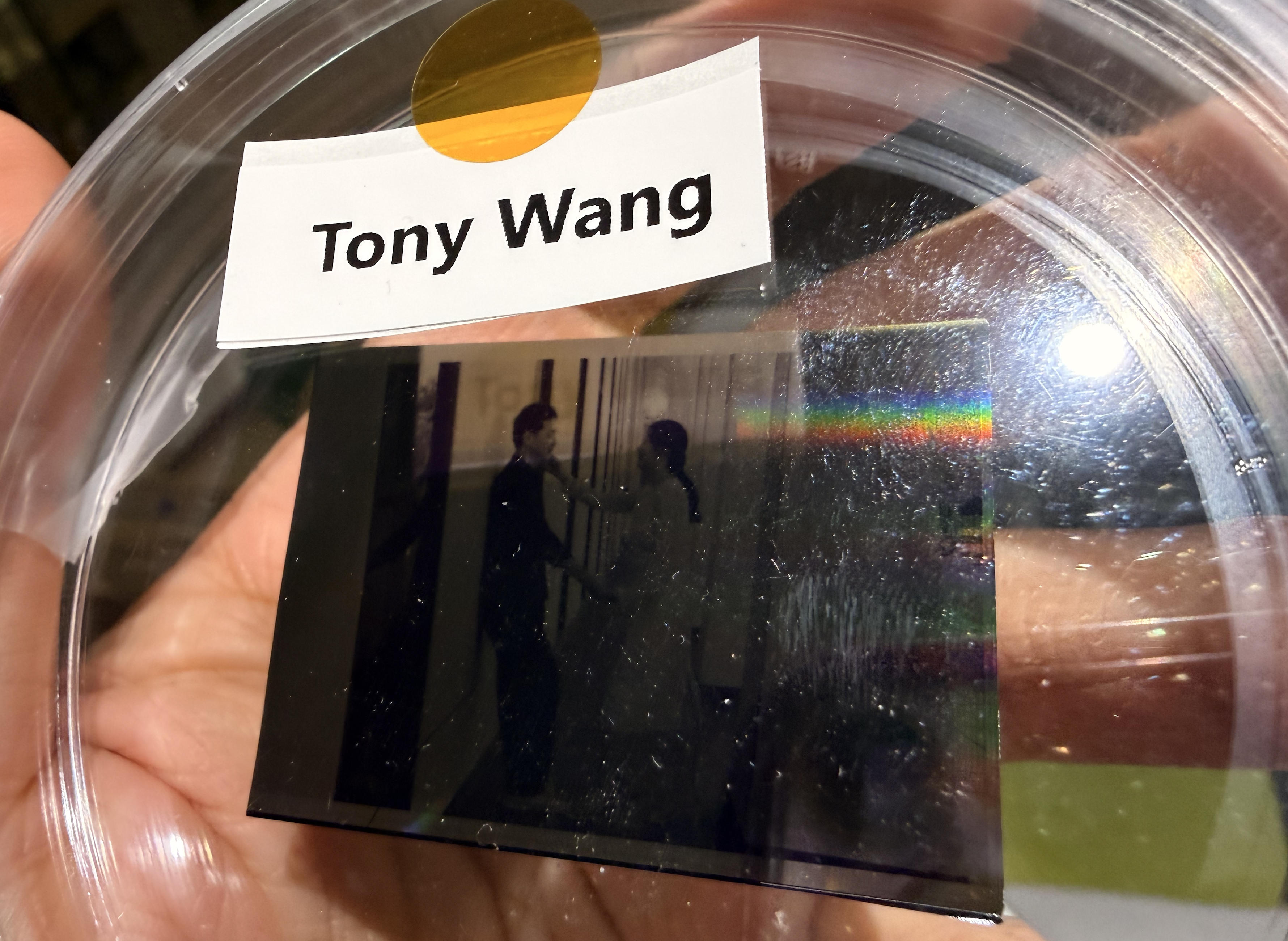
I walk past the MIT.nano building very often, and one of the things that always catches my eye is this One.MIT project: a permanent display tucked into a quiet corner of MIT.nano. At the time of this writing, there are two disks on display. On the newer and larger disk, nearly 340,000 names of MIT alumni, faculty, and students have been densely etched onto a surface no larger than a DVD.
In addition, there's a similar disk on display at the MIT Museum, paired with an interactive setup that helps visitors find their names if they're part of the MIT community—which is pretty cool.
One interesting detail is that the cutoff date for the names is 2024, before I attended MIT. Yet I was still able to find my name (on the disk displayed at the Museum, that is—there's no way to visually distinguish individual letters at the nanoscale). I imagine this means that identical names are only etched once, and as it happens, I do know someone with my exact same name who graduated from MIT two years ago 😀
Inspired by that, I decided that among all the interesting options for this assignment, I would choose microfabrication and try to "draw" an image on a disk in a similar way.
Understanding Silicon Wafers
Wafer: A thin, flat, ultra-pure substrate mostly made of silicon (~95% of the semiconductor industry) used as the base for microfabrication and integrated circuits.
Why silicon?
- Semiconductor whose conductivity is tunable via doping
- Forms high-quality native oxide (SiO₂) for insulation
- Abundant and relatively low-cost
- Mechanically strong and thermally stable
- Supported by a mature industrial ecosystem
Dimension and Purity
- Thickness: ~500–800 µm (≈ credit card thickness)
- Diameter: 4", 6", 8", 12" (300 mm standard)
- Electronic-grade purity: 9N: 99.9999999% · 11N: 99.999999999%
- Clean rooms are essential: modern fabs operate at Class 1 or better (≤1 particle per cubic foot of air).
Why wafers are disk-shaped
- Cylindrical crystal growth → circular slices
- Rotation-based processes require symmetry:
- Spin-coating photoresist
- Uniform heating
- Centrifugal drying
- Symmetric chemical flow
- Disks coat evenly; squares cause edge buildup and stress
- Industry lock-in: $10–20B fabs optimized entirely for round wafers
Unused or defective regions
- Edge regions, damaged dies, and failed chips are scrapped
- Some material is recycled as raw silicon feedstock
- Crystal perfection cannot be restored → never reused as wafers
Standard Microfabrication Flow
Sourced from ChatGPT and other online sources and reorganized here.
- Start with a wafer: Clean, inspect, and prepare a single-crystal silicon wafer.
- Form base films: Grow or deposit thin layers (e.g., SiO₂, Si₃N₄, polysilicon, metals).
- Coat with photoresist: Spin-coat liquid resist and soft-bake to form a uniform film.
- Pattern by lithography: Align the mask, expose with UV light, and develop the resist to create a pattern.
- Etch or modify material: Use wet or dry etching to transfer the pattern into the underlying film, then strip the resist.
- Doping: Introduce dopants by ion implantation and activate them with thermal annealing.
- Repeat for multiple layers: Alternate film deposition, lithography, etch, and doping to build transistors and interconnects.
- Planarize: Use chemical mechanical polishing (CMP) to flatten surfaces for further processing.
- Passivation: Deposit protective layers and open contact windows over bond pads.
- Wafer test: Electrically test each die on the wafer and map good versus bad chips.
- Dicing: Saw or laser-cut the wafer along scribe lines to separate individual chips.
- Packaging and final test: Attach dies to packages, connect them (wire bond or flip-chip), encapsulate, and perform final electrical tests.
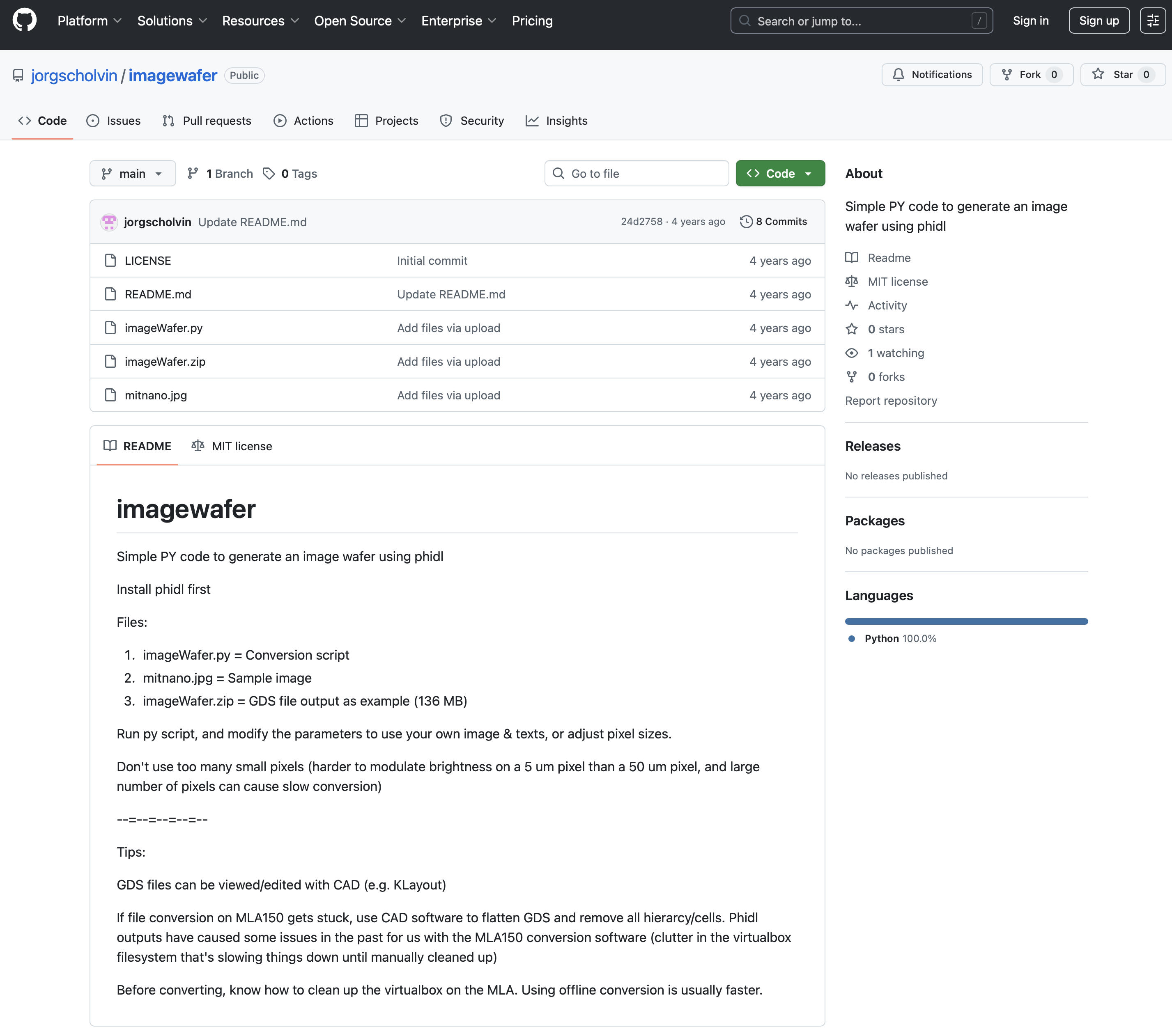
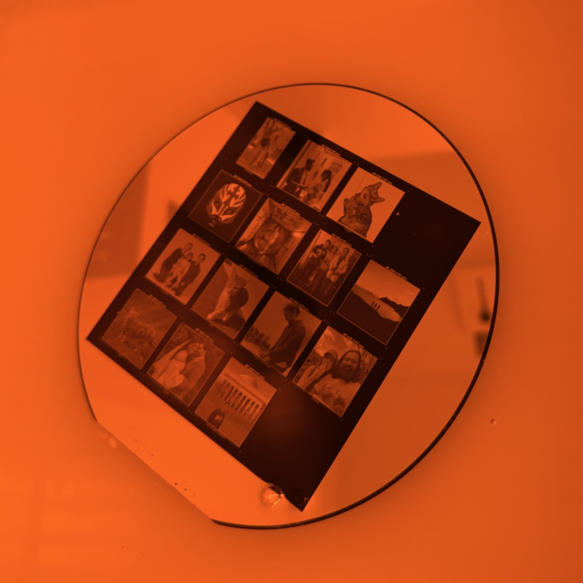
I'm using the open-source imagewafer project to convert a bitmap image into a GDSII layout using Python and PHIDL. The link to the site is here: imagewafer GitHub repository .
Goal: Take an image (like mitnano.jpg) and convert it into a GDSII layout made of tiny "pixels" (rectangles or shapes) that you can write on a wafer using tools like the MLA150.
Toolchain:
- phidl – a Python library for creating GDS layouts (often used with KLayout, lithography, photonics, etc.).
-
imageWafer.py – a ready-made Python script that:
- Loads the image.
- Converts it into a grid of pixels.
- Turns each pixel into geometry in a GDS file.
- Optionally adds some text.
-
Output:
imageWafer.gds(or similar) → can be sent to the MLA150 or viewed in KLayout.
I did have to install the phidl library first. I used pip to install it in my Python environment:
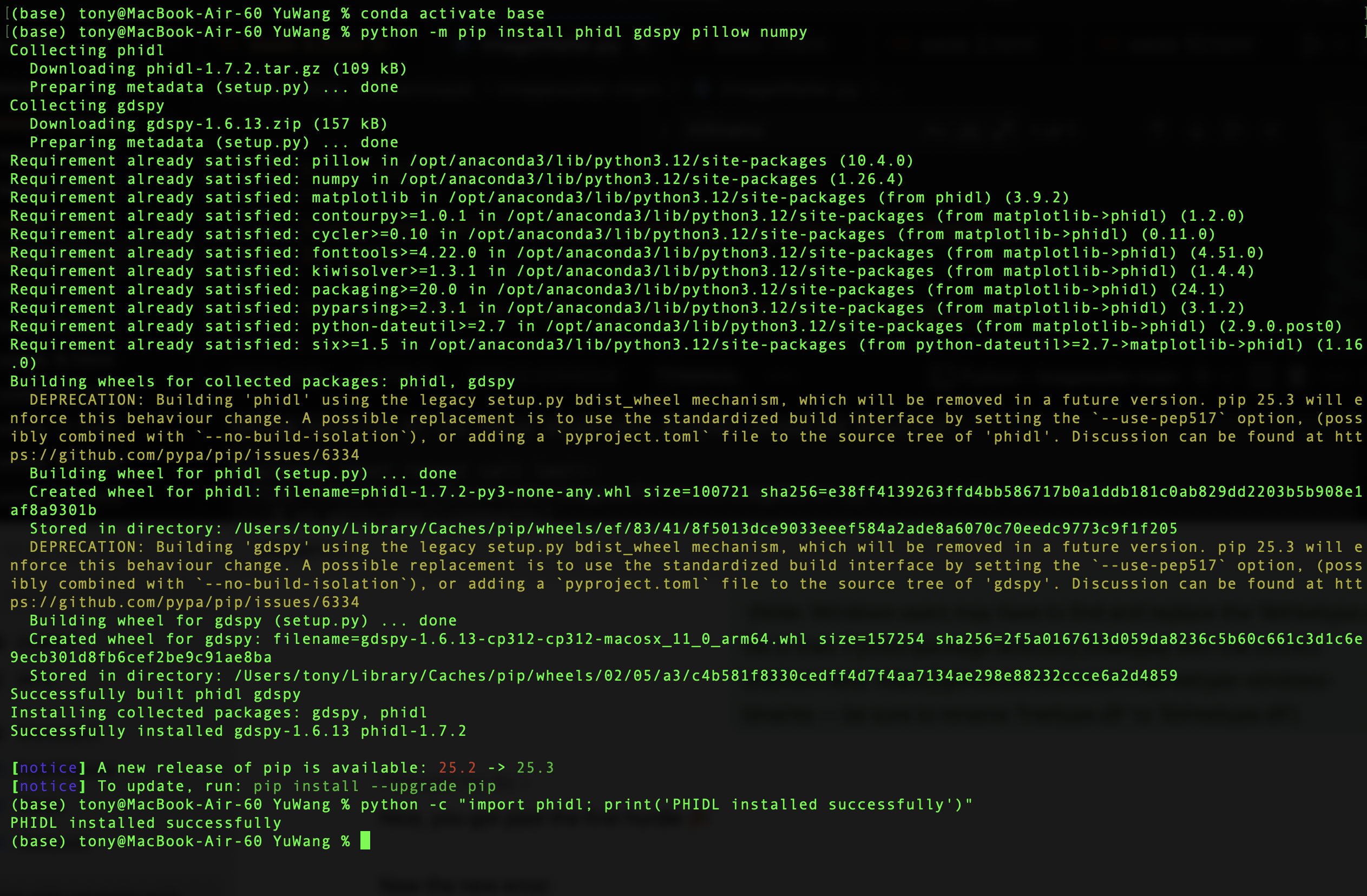
When I first run the code there were error reporting, after some investigation, it appears to be the issue of a font library. I made changes in the code to change the font setting from "Calibri" to "DEPLOF", which is PHIDL's default font, and the export succeeded!
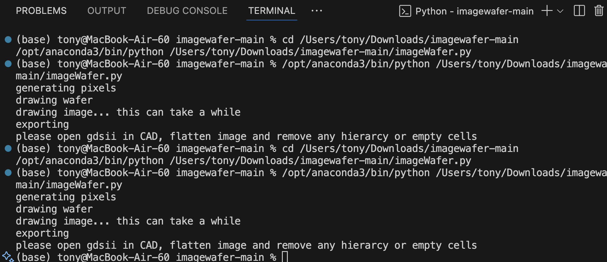
This is the code I used to make the final conversion. I modified the code I downloaded from the open-source imagewafer project. Changed a few parameters, including the default font and the file path used to load photo/pictures.
Unfortunately I don't have lab access, so I sent the converted file to Aijia and asked her to do it for me. The file was big, around 170MB!
Results

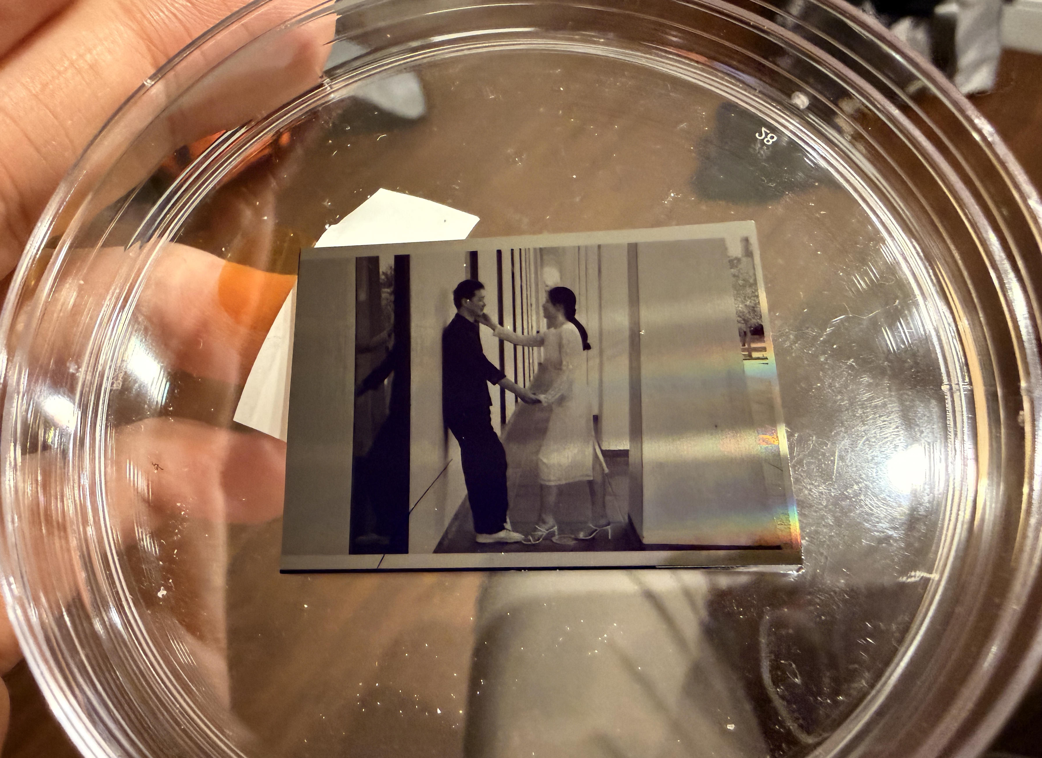
Since a wafer is made of silicon and is, at its core, refined sand, looking at this immediately reminded me of William Blake's Auguries of Innocence.
To see a world in a grain of sand
And a heaven in a wild flower,
Hold infinity in the palm of your hand
And eternity in an hour.A robin redbreast in a cage
Puts all Heaven in a rage.
A dove house fill'd with doves and pigeons
Shudders Hell thro' all its regions.
A dog starv'd at his master's gate
Predicts the ruin of the state.
A horse misus'd upon the road
Calls to Heaven for human blood.
Each outcry of the hunted hare
A fibre from the brain does tear.
A skylark wounded in the wing,
A Cherubim does cease to sing.
The game cock clipp'd and arm'd for fight
Does the rising Sun affright.
Every wolf's and lion's howl
Raises from Hell a human soul.…
He who respects the infant's faith
Triumphs over Hell and Death.
The child's toys and the old man's reasons
Are the fruits of the two seasons.
The questioner, who sits so sly,
Shall never know how to reply.
He who replies to words of doubt
Doth put the light of Knowledge out.Every night and every morn
Some to misery are born.
Every morn and every night
Some are born to sweet delight.
Some are born to sweet delight,
Some are born to endless night.God appears and God is light
To those poor souls who dwell in night,
But does a human form display
To those who dwell in realms of day.
Update: January 12, 2026
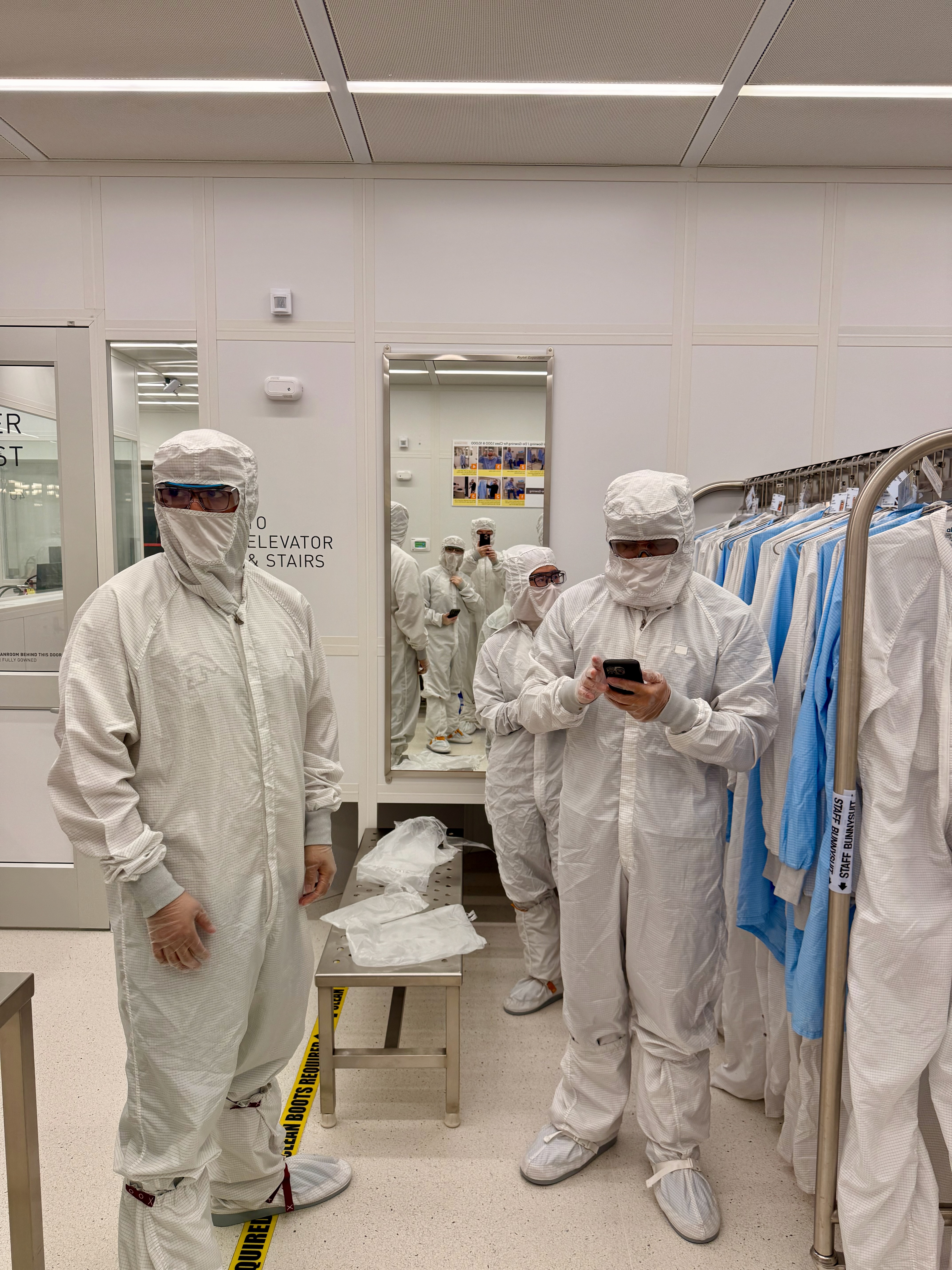
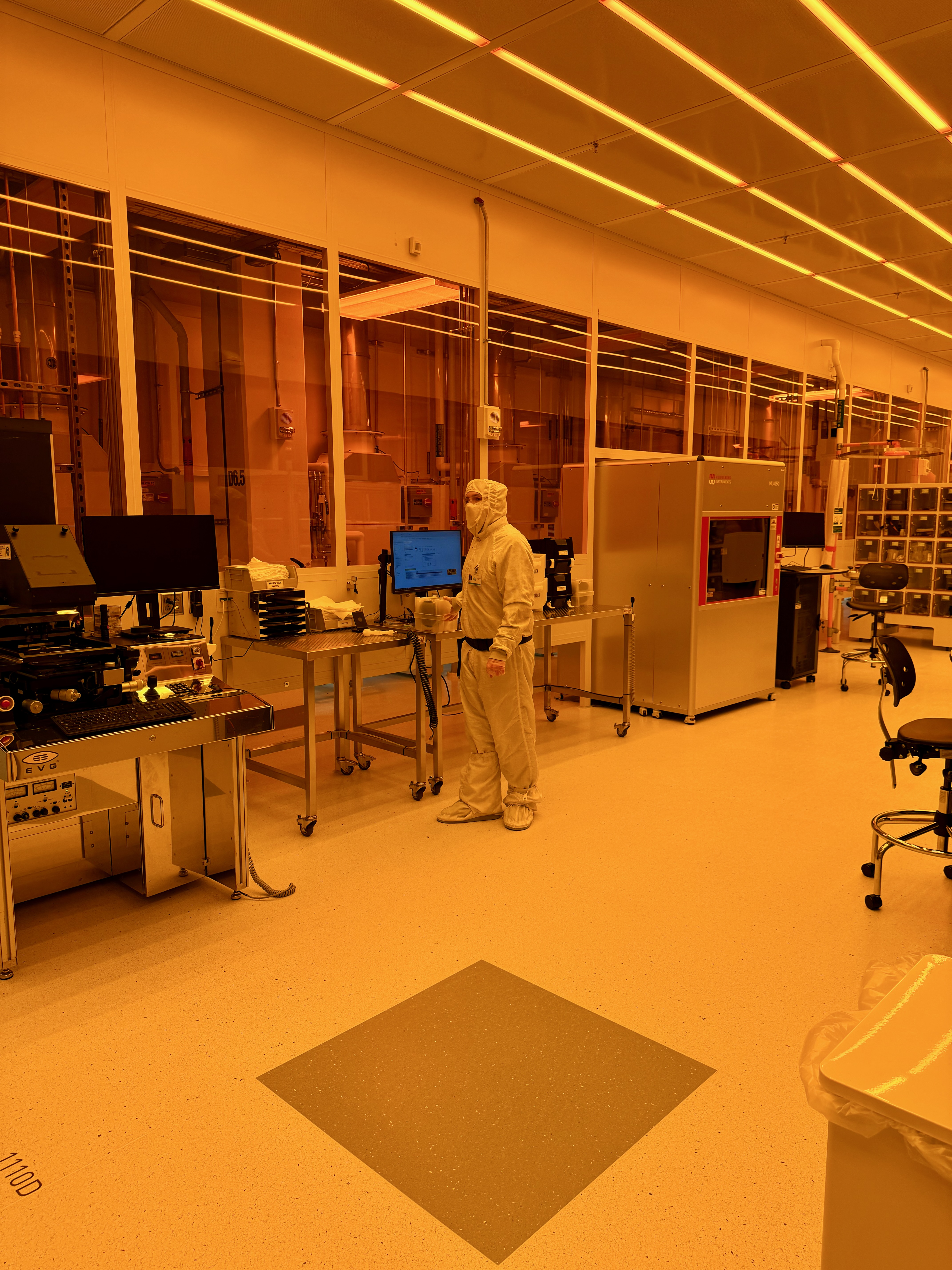
Today I went to Nano building to do a microfabrication myself. In the previous work I only convert the GDSII file and Aijia did the fabrication for me, which is why I am so inclined to sign up for an IAP activity during winter break and really get into the clean room in Nano building this time with a few friend of mine.
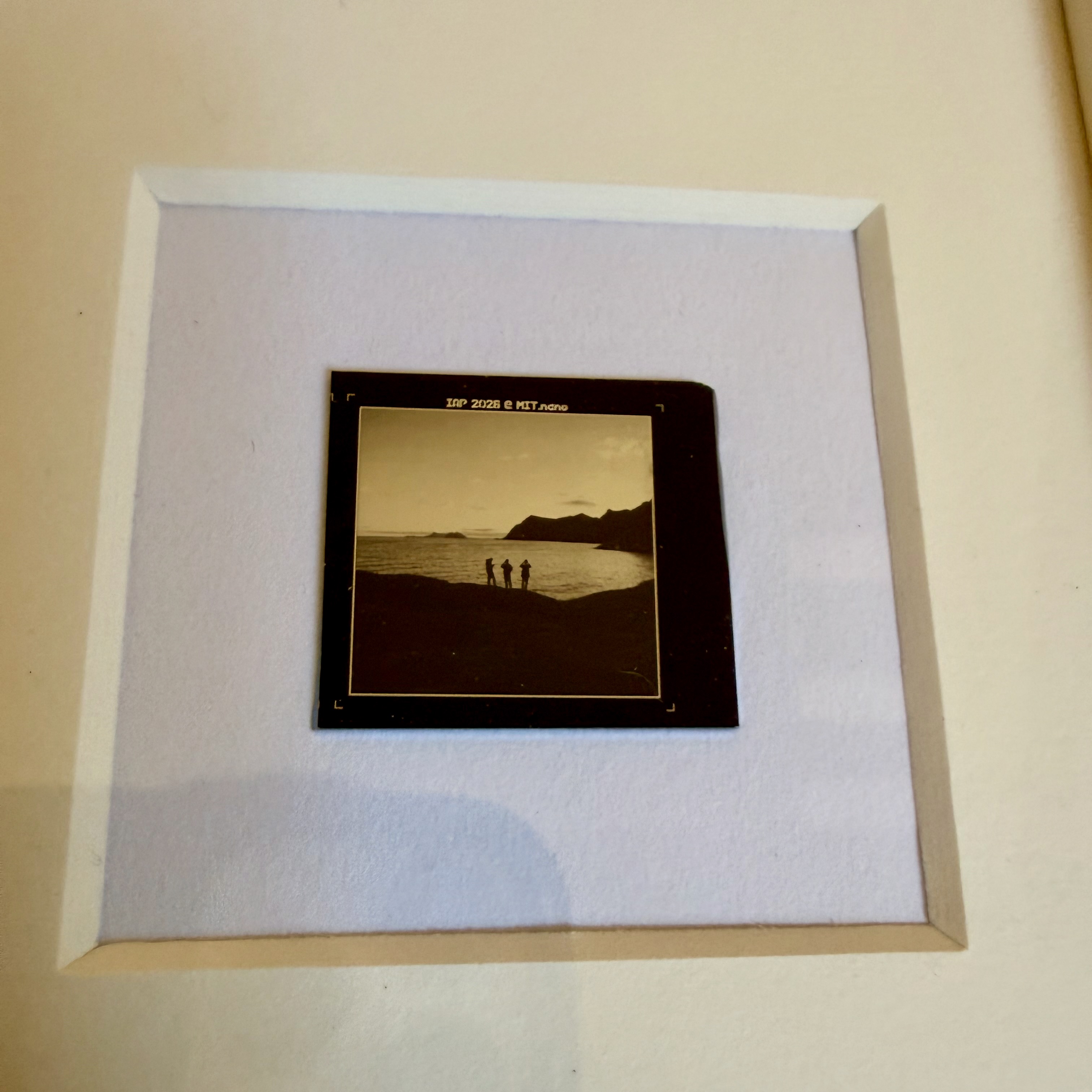
I am using a photo that I took in 2017 when I travelled to Lofoten, Norway.